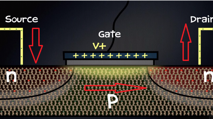
In the mobile phone, there are nearly 100 million transistors, in the computer, there’s over a billion. The transistor is in virtually every electronic device we use: TV’s, radios, Tamagotchis. But how does it work? Well, the basic principle is actually incredibly simple. It works just like this switch, so it controls the flow of electric current. It can be off, so you could call that the zero state or it could be on, the one state.


And this is how all of our information is now stored and processed, in zeros and ones, little bits of electric current. But unlike the switch, a transistor doesn’t have any moving parts. And it also doesn’t require a human controller. Furthermore, it can be switched on and off much more quickly than a human can flick this switch. And finally, and most importantly it is incredibly tiny. Well, this is all thanks to the miracle of semiconductors or rather the science of semiconductors. Pure silicon is a semiconductor, which means it conducts electric current better than insulators but not as well as metals. This is because an atom of silicon has four electrons in its outermost or valence shell. This allows it to form bonds with its four nearest neighbors. So it forms a tetrahedral crystal.

But since all these electrons are stuck in bonds, few ever get enough energy to escape their bonds and travel through the lattice. So having a small number of mobile charges is what makes silicon a semiconductor. Now, this wouldn’t be all that useful without a semiconductor’s secret weapon – DOPING. You’ve probably heard of doping, it’s when you inject a foreign substance in order to improve performance. There are two types of doping called n-type and p-type.

To make n-type semiconductor, you take pure silicon and inject a small mount of an element with 5 valence electrons, like Phosphorous. This is useful because Phosphorous is similar enough to silicon that it can fit into the lattice, but it brings with it an extra electron. So this means now the semiconductor has more mobile charges and so it conducts current better. In p-type doping, an element with only three valence electrons is added to the lattice. To make n-type semiconductor, you take pure silicon and inject a small mount of an element with 5 valence electrons, like Phosphorous. This is useful because Phosphorous is similar enough to silicon that it can fit into the lattice, but it brings with it an extra electron. So this means now the semiconductor has more mobile charges and so it conducts current better. In p-type doping, an element with only three valence electrons is added to the lattice.
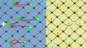
Now, this creates a ‘hole’ – a place where there should be an electron, but there isn’t. But this still increases the conductivity of the silicon because electrons can move into it. Now although it is electrons that are moving, we like to talk about the holes moving around – because there’s far fewer of them. Now since the hole is the lack of an electron, it actually acts as a positive charge. And this is why p-type semiconductor is actually called p-type. The p stands for positive – it’s positive charges, these holes, which are moving and conducting the current. Now it’s a common misconception that n-type semiconductors are negatively charged and p-type semiconductors are positively charged. That’s not true, they are both neutral because they have the same number of electrons and protons inside them. The n and the p actually just refer to the sign of charge that can move within them. So in n-type, it’s negative electrons which can move, and in p-type it’s a positive hole that moves. But they’re both neutral! A transistor is made with both n-type and p-type semiconductors.
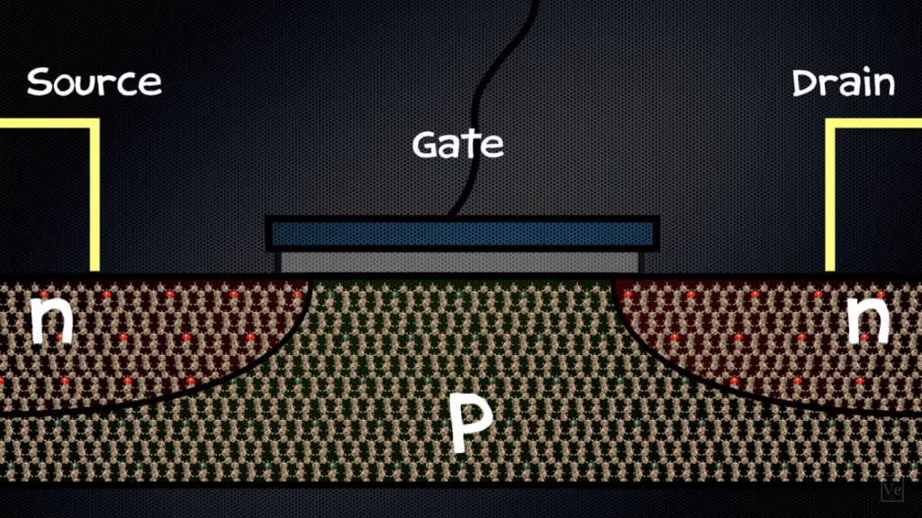
A common configuration has n on the ends with p in the middle. Just like a switch, a transistor has an electrical contact at each end and these are called the source and the drain. But instead of a mechanical switch, there is a third electrical contact called the gate, which is insulated from the semiconductor by an oxide layer. When a transistor is made, the n and p-types don’t keep to themselves – electrons actually diffuse from the n-type, where there are more of them into the p-type to fill the holes. This creates something called the depletion layer. What’s been depleted?
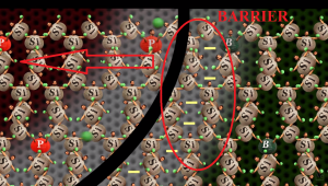
Charges that can move. There are no more free electrons in the n-type. Why? Because they’ve filled the holes in the p-type. Now this makes the p-type negative thanks to the added electrons. And this is important because the p-type will now repel any electrons that try to come across from the n-type. So the depletion layer actually acts as a barrier, preventing the flow of electric current through the transistor. So right now the transistor is off, it’s like an open switch, it’s in the zero state.

To turn it on, you have to apply a small positive voltage to the gate. This attracts the electrons over and overcomes that repulsion from the depletion. It actually shrinks the depletion layer so that electrons can move through and form a conducting channel. So the transistor is now on, it’s in the one state. This is remarkable because just by exploiting the properties of a crystal we’ve been able to create a switch that doesn’t have any moving parts, that can be turned on and off very quickly just with a voltage, and most importantly it can be made tiny. Transistors today are only about 22nm wide, which means they are only about 50 atoms across. But to keep up with Moore’s law, they’re going to have to keep getting smaller. Moore’s Law states that every two years the number of transistors on a chip should double. And there is a limit, as those terminals get closer and closer together, quantum effects become more significant and electrons can actually tunnel from one side to the other. So you may not be able to make a barrier high enough to stop them from flowing. Now this will be a real problem for the future of transistors, but we’ll probably only face that another ten years down the track.